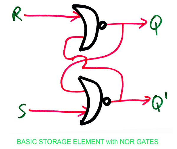
Fast state storage is based on the inverting gate loop. The basic NOR storage element is shown below:
(Q)Trace the operation of this circuit as RS are cycled from 01 to 00 to 10 to 00.
(Q)Explain the issue of metastability in this circuit.
This basic storage element in reality is more likely to be implemented with NAND gates, owing to the slightly greater overall speed of NAND in silicon CMOS technology. However, the NOR version is a bit more intuitive in its tracing of operations, as its changes occur with active high inputs on R and S.
Since it has two inputs, it is a bit awkward for data storage, so it makes sense to add an inverter to create the complementary inputs.
(Q)Why can't we simply slap an inverter from S to R?
The improved circuit is called the D latch and is shown below:

The most significant thing here is the addition of the ENABLE input; if low, the latch is closed; both R and S inputs are 0, meaning that the storage element (the NOR gates) are storing a bit previously entered. If high, ENABLE opens the AND gates, allowing the D input to propagate through the NOR gates, forcing Q to follow D (and Q' to be the complement of D ). The latch is said to be "transparent" when ENABLE is 1. When ENABLE goes low, this new stored value will be preserved in the closed latch.
(Q)Is is possible for the D latch to show metastability? If so, explain the sequence of events that will trigger it.
The D latch allows a minimal method of controlling data movement through a computing device; however, the time that ENABLE is allowed to be high must be carefully controlled in order to prevent a "race condition" in which data can move through one latch and into another latch elsewhere in the system, owing to the transparency of the latches.
This problem can be completely solved through the use of the edge-triggered "flip flop". The logic design notes show the design for one of these; however I will show the master-slave device here.
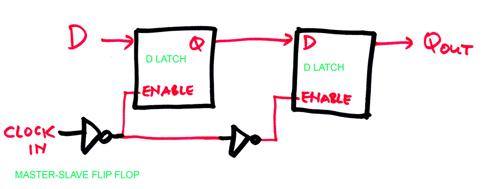
This prevents races by never being transparent. A bit is fully propagated from D input to Q output only after a complete cycle of the clock control line. I have shown two inverters on CLOCK; this allows positive edge triggering; that is, the Q output is updated just after the clock transitions from 0 to 1.
(Q)Explain the operation of the master-slave device.
(Q)Is metastability an issue? Explain.
MANO2: p 202-214 I HATE his terminology!
MANO3: p 167-175 He uses better terminology in this edition!
The final step in the design of our data storage device to allow a complete computer to be easily realized is the fully synchronous flip flop device for data transfer. If we construct a system in which the clock runs continuously and hits all flip flops in the system continuously, we have a fully synchronous system. This is very nice in which the basic computer design becomes a lot like plugging together LEGO blocks. If a few simple rules are followed, the system is guaranteed to work; the only constraint being that the clock speed must not exceed a certain value, dependent on the technology used.
[Because of the relative complexity of the full flip flop compared to the basic storage element, it should be no surprise that in the early days of computers, using vacuum tubes or discrete transistors, fully synchronous implementations were not done.]
The fully synchronous system is not without issues; it requires a more complex basic circuit (more transistors); the continuous operation of the clock to all parts of the system increases power consumption, especially in CMOS, and the need to use a fixed speed clock means that the system has to run at the speed of the slowest speed part of it. All of these have kept interest in "asynchronous" architectures alive. In practice, however, a fully asynchronous system seems to be unattainable; the problem of races is virtually insurmountable without handshaking schemes which would seem to slow things down almost as much as the fixed clock does.
I will also note that the naive designer will typically tend to design an asynchronous system; it seems intuitive to store data in latches, with individual clock pulses directed to those latches that need to store new data. Unfortunately, it is very difficult to guarantee correct operation; there is the race problem, and also the problem of keeping noise spikes or "runt pulses" off the clock or enable input to the latch. The fully synchronous system solves these problems but is definitely not as intuitive for the student at first.
Anyway, we finally come to what I call the "basic LEGO block" of a synchronous computer system:

The clock runs continuously for all flip flops in a fully synchronous system, as mentioned. Control of data flow is accomplished by the use of the LOAD inputs. The nice thing about this circuit is that any input can have noise spikes on it; only the clock must be clean. If the clock is running continuously, this is relatively easy to achieve. The only contraint is that the set up and hold times for the D input on the flip flop itself must be observed, and this is also easy if the clock runs slowly enough.
So, if we wish to maintain the current contents of the bit, we keep LOAD at 0 close to the clock edge (we don't care about it at other times, as no action is taken except when the clock edge arrives). Thus, when the clock edge does arrive, the old data is recirculated back to D and re-transferred to Q. This occurs on each clock edge until we wish to load new data.
(Q)Trace the storage methods from basic storage element through latch, flip flop and synchronous bit storage. Explain how each represents an improvement over its prececessor. Explain the basic principle of operation of each.
The above diagram might be considered a "one-bit slice" of a data storage "register". If we were to take 32 of the above units, connect the LOAD signals all together, and run the whole thing off the same clock, we would have a "static 32-bit register". The "static" comes from the fact that it retains its data indefinitely until LOAD goes to 1 and new data is entered. [Also, even if the clock is stopped, the flip flops retain their data indefinitely, so long as power is supplied. The main other technology, "dynamic" storage, requires some sort of external circuits to continually reload ("refresh") the data. In a dynamic system, stopping the clock will normally result in loss of data after a few milliseconds.]
MANO2: p 258-262.
MANO3: p 217-221.
We can extend this idea to construct a multifunction register as shown:

The output of the register will be determined by the values of the control inputs when the clock edge arrives. Note that the incrementer is just a daisy chain of half adders; a half adder is just an XOR gate and an AND gate. The incrementer and decrementer are basically the same thing; if the Q' output of the flip flop is fed into an incrementer, we get decrementing happening. This whole thing of course is repeated for each bit; a 32 bit register would need 32 copies of all the logic shown. The incrementer and decrementer will span all 32 bits, as they involve carries.
Another function we might find useful would be SHIFT; [you know: shift happens] this is accomplished simply by connecting bit i to bit i+1 for a left shift, and vice versa for a right shift. We can connect these through the MUX to make the functionality selectable.